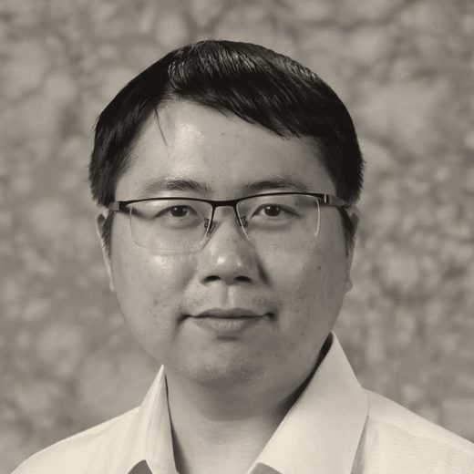


Dr. Suman Datta
Co-inventor of Intel's High-k/Metal Gate and 3D Tri-Gate transistors, the breakthroughs that carried computing from 45 nm to today. Recipient of the 2026 IEEE Andrew S. Grove Award. Pettit Chair Professor, Georgia Tech.
Z2RAM · memory on compute
No capacitor. No interposer. No trip off the chip. Z2RAM is fast enough to keep compute saturated, dense enough to hold weights and KV cache, and built for the power and thermal budget of a multi-kilowatt accelerator.
Memory is the most critical hardware bottleneck standing in the way of AI innovation. The more data has to move, the more time and energy it consumes… and costly processors sit idle for longer. Surging AI workloads and an evolving infrastructure demand a new memory tier that combines high speed with high capacity to improve response times, lower costs, and maximize efficiency.
Current memory architectures create tradeoffs that hyperscalers and modern AI systems can no longer afford. SRAM keeps data close, but runs out of capacity almost immediately. HBM and DRAM hold more, but are located off-chip, creating steep latency penalties and energy waste. Fetching a number from HBM takes roughly 1,000× more energy than operating on it.
Z2RAM is Nagare Labs' answer: a memory with SRAM-class speed at DRAM-class density, designed from the start to sit directly on the AI accelerator.
Bandwidth, latency, and energy per bit are all excellent. Capacity is not: six transistors per bit, half the die, and no longer shrinking.
Intricately and expensively stacked beside the accelerator, connected by a few thousand lanes through an interposer. Every bit pays for the trip in energy, and every access pays for it in latency.
Conventional DRAM bonded onto the accelerator recovers much of what SRAM offers. But DRAM has to stay below about 95 °C, which throttles the logic beneath it. So stacks stay short, most of the model goes back to the interposer, and each layer is a separate die to bond and yield.
A transistor-only cell built from oxide semiconductors, deposited in layers on one die. SRAM-class access, DRAM-class density, and stable at accelerator operating temperatures.
| Memory on compute requirements | SRAM | HBM | Stacked DRAM | Z2RAM | How we do it |
|---|---|---|---|---|---|
| Keep data next to computeNo interposer; hundreds of thousands of lanes, not thousands | Memory layers stacked directly over logic, with connections running vertically through every layer. Bits travel micrometers, not millimeters. | ||||
| Well under a pJ per bitFree the power budget for compute | No bumps or bonds between memory layers at all, and almost no energy spent holding data in place. | ||||
| Low latencySRAM-class access, no interface training | A fast, non-destructive read at SRAM-class access times, and refresh so infrequent it stays out of the way of the workload. | ||||
| Higher-temperature operationStable where conventional DRAM is not | Near-zero-leakage oxide-semiconductor transistors hold data at temperatures where conventional DRAM cells cannot, and draw far less power doing it. | ||||
| Scalable by designDeposited layers, not bonded dies | Z2RAM adds capacity by depositing another memory layer on the same die and patterning them all together, the way 3D NAND grew. One thin die with low thermal resistance. |
Access speed nearly on par with SRAM, so AI accelerators compute instead of wait.
projected at Gen 1More memory in less space, for larger models and longer context, with a roadmap past 10× as layers are added.
projected at Gen 1Lower power and heat, with no refresh cycles burning energy to hold data in place.
projected at Gen 1Past attempts at a new memory stalled on exotic materials or physics that scaled poorly. Z2RAM rests on three breakthroughs, each proven on its own and combined for the first time in a cell that meets the needs of AI infrastructure.
Eliminating the capacitor ceiling.
Conventional DRAM relies on microscopic capacitors that are hitting physical scaling limits and drain their charge when read. Z2RAM stores data in transistors alone, delivering fast, non-destructive reads and bypassing the capacitor manufacturing wall entirely.
Eliminating constant refresh.
Silicon transistors leak faster as accelerator junction temperatures rise, burning energy just to keep stored bits alive. Z2RAM's oxide-semiconductor channel cuts off-state leakage by orders of magnitude, so data holds far longer between refreshes.
Eliminating the interposer bottleneck.
Instead of stacking separately bonded DRAM dies beside the chip, Z2RAM deposits its memory layers on a single die with standard 300 mm processes and joins it directly to the accelerator. Capacity scales vertically, without node shrinks or EUV.
Z2RAM is designed to scale efficiently with existing materials, fab nodes, and 300 mm production-class tooling. It is stacked memory at array scale with the same tools and chemistries fabs already run. Production can scale with foundry and packaging partners rather than being limited to a factory of our own. That is the difference between memory that can be made and memory that can be made in volume.
For most of their careers, Suman Datta and Shimeng Yu advised the memory industry from the outside. Suman's transistors are in nearly every processor shipping today. Shimeng's simulator is how the industry decides which memory to build. When their own lab's results crossed from promising to buildable, they got off the sidelines and founded Nagare Labs to build it themselves.
Co-inventor of Intel's High-k/Metal Gate and 3D Tri-Gate transistors, the breakthroughs that carried computing from 45 nm to today. Recipient of the 2026 IEEE Andrew S. Grove Award. Pettit Chair Professor, Georgia Tech.
Creator of NeuroSim, the industry standard for modeling emerging memory and AI hardware, used by foundries and chip designers worldwide. Dean's Professor, Georgia Tech; PhD, Stanford.
Suman Datta's IEEE Micro perspective proposes back-end-of-line oxide-semiconductor transistors for monolithic 3D integration.
First amorphous-oxide two-transistor gain cell demonstrated at IEDM.
Core material and device structure selected; device reliability optimized (VLSI).
Memory bit cell experimentally demonstrated (IEDM); four-layer stacked transistor structure fabricated. Shimeng Yu's group publishes the thermal and power-delivery analysis of HBM stacked on logic that quantifies stacked DRAM's ceiling (IEEE JxCDC).
Long-term stability shown (VLSI). Nagare Labs founded, with a clean institutional license from Georgia Tech and backing from Playground Global.
Guided by former leaders from Intel, Intel Foundry, and TSMC, and backed by Playground Global.
Former CEO of Intel and VMware. Intel's first CTO, architect of the 80486, and a semiconductor industry leader for four decades.
Former Senior Vice President and General Manager of Intel Foundry Technology Research and Development, responsible for Intel's leading-edge process technology.
Endowed Chair Professor at Stanford University and former Vice President of TSMC. Member of the National Academy of Engineering and a founding figure in emerging memory.
Coverage, press releases, and updates from Nagare Labs.
Nagare Labs announces its emergence from stealth and introduces Z2RAM, a memory architecture designed to address AI's memory bottleneck.
Read press release →The Register reports on Pat Gelsinger's backing of Nagare Labs and its Z2RAM memory architecture, exploring its potential for AI infrastructure and the challenges ahead.
Read coverage →Accelerator and system designers, foundries, and packaging partners. If you are putting memory on top of compute, we should talk.
Start a conversation →A founding team of device, process, and memory-design engineers. Small team, hard problem, direct line from your work to the silicon.
See open roles →Nagare Labs is backed by Playground Global. If you invest in the future of AI infrastructure and want to follow our progress, we'd like to hear from you.
Get in touch →Every early hire shapes the architecture, the process, and the company.
| Role | What you'll own | Background we're looking for |
|---|---|---|
| Device & Process Integration Engineer | Oxide-semiconductor transistor and 3D module development on 300 mm tooling | Thin-film or BEOL integration; DRAM or 3D NAND process background |
| Memory Circuit Designer | Array, sense, and peripheral design for stacked memory | DRAM or eDRAM core design; tape-out experience |
Atlanta, GA, with flexibility for the right candidates. Write to hello@nagarelabs.ai.